
Semiconductor manufacturing has traditionally followed a linear innovation model. New tools and processes are developed in silos, each optimized for its step in the chipmaking journey. But that separation is beginning to fade. Today’s most challenging performance demands reveal the need for deep collaboration between previously distinct domains. A prime example is the growing constructive collaboration between lithography and etch technologies. Erik Hosler, a strategist who connects semiconductor advancements with cross-industry dynamics, highlights that progress can no longer be confined to isolated improvements.
This shift toward process integration is redefining what it means to innovate. Rather than pushing lithography or etch independently, engineers are now developing strategies where both develop together. This coordinated approach allows for greater control, improved precision, and smarter use of design space. As chip architectures grow more complex and feature sizes shrink further, the industry is discovering that breakthroughs are more likely when tools work together rather than alone.
Lithography Sets the Pattern, Etch Seals the Deal
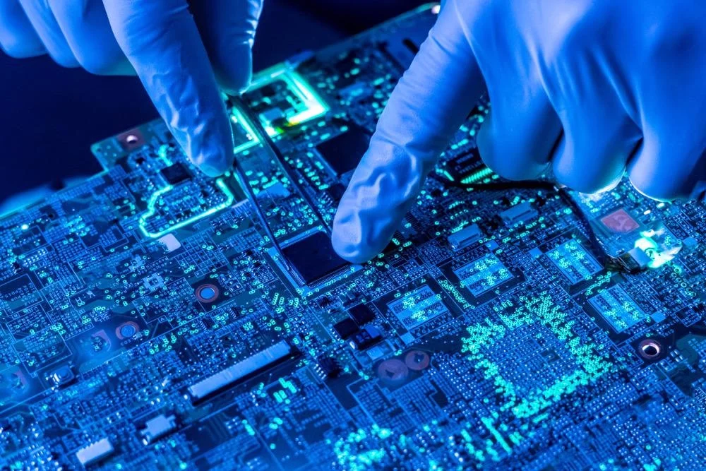
Lithography has always been seen as the blueprint of semiconductor design. It defines the pattern that can become the electrical pathways and logic elements of a chip. But patterning is only part of the story. Once the photoresist is exposed and developed, those patterns must be etched into the underlying material. That is where the etch process takes over.
At advanced nodes, small distortions or shifts in the resist can lead to significant variation in the final etched feature. Even perfectly printed patterns can be distorted during the etch step if not carefully managed. That is why lithography and etch must be co-optimized. When their capabilities and constraints are jointly understood, the result is more accurate, reproducible, and scalable.
This collaboration is particularly crucial in 3D structures such as finFETs and gate-all-around transistors. These designs require precision not just across the horizontal plane but through the vertical axis. Small deviations in etch angle or depth can undermine the electrical properties of the entire structure.
From Handoff to Handshake
Historically, lithography teams and etch engineers worked in sequential stages. Lithography handed off its pattern, and etch took it from there. This handoff model worked when design tolerances were broad. But in today’s environment of atomic-scale features, that model is no longer sufficient.
Manufacturers are now shifting toward what could be called a handshake model. Etch and lithography are treated as a single integrated process, with shared responsibility for pattern fidelity. Toolmakers are collaborating across disciplines to ensure compatibility and joint optimization.
A notable example of this shift came during a plenary presentation at SPIE’s Advanced Lithography symposium, where ASML and Lam Research discussed their work on integrated 3D patterning solutions. Their message was clear. Delivering next-generation performance requires tighter alignment between exposure and etch.
Innovation Through Cross-Process Feedback
Joint development does not stop with equipment integration. It extends into shared data, modeling, and control strategies. Advanced Process Control (APC) systems now collect data from both lithography and etch steps, using AI-driven analytics to adjust parameters dynamically.
Engineers can use this feedback loop to predict how a resist profile can respond during etch and adjust the lithography pattern accordingly. Similarly, the etch process can be tuned to account for variations in exposure or focus, effectively smoothing out imperfections before they become defects.
Erik Hosler notes, “It’s going to involve innovation across multiple different sectors.” This kind of innovation is not limited to fabrication floors. It draws on physics, chemistry, materials science, and computer modeling. The convergence of these disciplines allows fabs to move beyond one-size-fits-all solutions and toward custom process stacks tailored to specific applications.
Shared Goals, Aligned Roadmaps
The growing connection between lithography and etch is influencing how technology roadmaps are developed. In the past, each function followed its trajectory. Lithography focused on light sources and optics, while the etch team worked on plasma chemistry and chamber design.
Now, those trajectories are being braided together. When one process changes, the other must adapt. For example, the shift to high-NA EUV lithography requires new resist materials with different etch characteristics. Likewise, innovations in directional plasma etching must be coordinated with mask design strategies to ensure alignment and resolution.
This alignment reduces risk and speeds up development. It also makes it easier to evaluate tradeoffs. If a more aggressive etch process enables simpler patterning or if a smarter exposure reduces the need for complex etch compensation, then both sides can benefit. Collaboration becomes a multiplier of capability.
Benefits Beyond Performance
Integrated process development improves technical performance and delivers economic and operational advantages. Co-optimization can reduce overall process steps, lower defect rates, and improve yields. It can also accelerate time-to-market. When lithography and etch teams share development cycles, design iterations become more efficient. Engineers can quickly evaluate new patterning schemes, assess results across both processes, and refine techniques without extensive rework.
This efficiency is critical in an era where market windows are shrinking and customization is increasing. Foundries and design houses need the flexibility to pivot quickly while maintaining quality and consistency.
A Model for the Future
The collaboration between lithography and etch is becoming a template for broader integration across the semiconductor value chain. Similar partnerships emerge between deposition and metrology, between packaging and logic design, and between system architects and materials developers.
As device complexity grows, no single team or discipline can drive innovation alone. Success depends on systems thinking, shared data, and open collaboration across previously disconnected silos.
The lithography-etch partnership is a compelling example of this future. It shows that when technologies meet not at the endpoint but at the idea stage, possibilities multiply. The rules are no longer written by one tool or one team. They are rewritten together.
Stronger Together
Individual advancements cannot power the next generation of semiconductor technology. It can be built through partnerships that cross technical, organizational, and disciplinary boundaries. Lithography and etch, once separate steps in a rigid process, are now forming a dynamic collaboration. Together, they are redefining how patterns are created, transferred, and perfected. This union is a model of modern development, which is responsive, adaptive, and integrated.
As the industry continues to face shrinking tolerances and rising complexity, the future can belong to those who align their tools, strategies, and goals. In doing so, they cannot only extend Moore’s Law but also redefine what progress looks like.


